Test & Measurement
Welcome to Electronic Design's destination for test and measurement technology trends, products, industry news, new applications, articles and commentary from our contributing technical experts and the community.
Recent
Recent
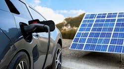
Dreamstime_akaratphasura_132202211

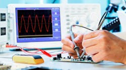
Dreamstime_melpomenem_159265108


Highlights
Highlights
66050573 © Nils Ackermann | Dreamstime.com

Sponsored Content
Fluke Calibration
Dreamstime_pojoslaw_305383108


Keysight and Dreamstime_lescunliffe_23231826
Andrei Dzemidzenka, Dreamstime
Dreamstime_ekkalucksangkla_1082822391

Electronic Design
Dreamstime_luchschen_26003212
Dreamstime_forfunlife_17805192
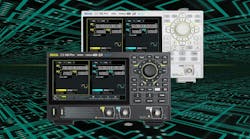
RIGOL Technologies